

Substantial Shunt Resistor Design Essentials for High-Accuracy Current Sensing
2026-07-12
Accurate current sensing is the linchpin of modern power electronics, but it often hinges on a tiny, overlooked component: the shunt resistor. Getting it wrong invites thermal drift, noise, and measurement errors that can derail your entire design. In this post, we strip away the guesswork and explore the non-negotiable design rules for substantial shunt resistors. Whether you're combating parasitic inductance or wrestling with thermal EMF, we'll walk you through the essentials—from material selection to layout—so your next sensing circuit delivers precision when it counts. Looking for robust, low-drift shunts? Check out Milliohm for solutions engineered for high-accuracy applications. Let's dive in.
Material science behind shunt resistor precision
The precision of a shunt resistor hinges critically on the choice of resistive alloy. Manganin, a copper-manganese-nickel alloy, remains a classic due to its near-zero temperature coefficient of resistance (TCR) around room temperature and exceptionally low thermal EMF against copper. Its stable microstructure, achieved through controlled cold working and annealing, minimizes resistance drift over time. However, for high-energy pulse applications, the alloy's moderate resistivity may lead to larger physical sizes, prompting the use of alternatives like Evanohm, which offers higher resistivity and superior strain tolerance, though at the cost of more complex manufacturability.
Beyond bulk composition, metallurgical imperfections and fabrication-induced stresses play a subtle but decisive role. Dislocations, grain boundaries, and microvoids scatter conduction electrons, raising noise and causing unpredictable resistance shifts under thermal cycling. Precision foil resistors address this by using etched, chemically stabilized alloys that undergo lengthy thermal preconditioning to relax internal stresses. The geometrical accuracy of the trimming process further ensures tight tolerance, but any residual mechanical strain from packaging or board flexing can modulate resistance through the piezoresistive effect, turning a precision device into a strain gauge if not carefully isolated.
The electrical contacts between the resistive element and its terminations form another materials frontier. High-quality shunts employ welded or brazed Cu-Mn-Ni terminals, avoiding tin-lead solder joints whose intermetallic growth introduces parasitic series resistance and thermoelectric offsets. In competitive designs, a deliberate mismatch in thermal expansion coefficients between the element and its mounting substrate creates a controlled compressive strain that counteracts the expected TCR, effectively flattening the resistance-temperature curve over a wider range. This marriage of metallurgy and mechanics exemplifies how deep material science transforms a simple strip of metal into a nearly invariant reference standard.
Geometry choices that minimize stray inductance
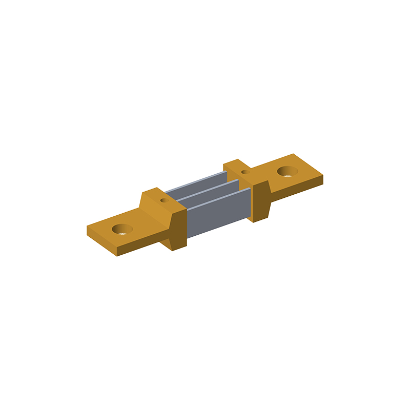
In high-frequency power circuits, the physical arrangement of conductors plays a decisive role in controlling stray inductance. Loop area is a primary factor; even a short, wide trace can introduce unwanted impedance if the return path is not tightly coupled. Designers often opt for a coplanar structure where the current-carrying trace runs directly above or adjacent to a ground plane, reducing the magnetic field loop. This approach confines the flux between layers, minimizing energy storage and thus parasitic inductance. Board stack-up also matters—placing power and ground planes next to each other, separated by a thin dielectric, creates an inherent low-inductance path for high-speed transients.
Component placement further influences stray magnetic coupling. Terminal-to-terminal proximity is critical; laterally arranging devices so that their current loops partially cancel can yield a significant drop in overall inductance. In DC-DC converters, for instance, positioning the input capacitors and switching transistors in a compact cluster keeps the high di/dt loop as small as physically possible. Tight grouping reduces not only the loop span but also the mutual inductance from parallel paths. Additionally, using wide, flat conductors instead of thin wires for high-current nodes distributes current more uniformly, lowering the partial inductance of each segment and mitigating local hot spots that can lead to voltage overshoot.
Another geometry-driven technique is the use of symmetrical and interleaved layouts. By splitting the current path into multiple paralleled layers or fingers, the net inductance drops because the magnetic fields from each branch partially subtract. This is evident in power module substrates where emitter and collector traces are interleaved in a finger pattern, effectively cancelling the opposing flux. Similarly, coaxial or quasi-coaxial arrangements—with an inner conductor fully surrounded by a return shield—deliver a nearly ideal low-inductance path. Such strategies demand careful attention to skin and proximity effects, but when applied judiciously, they can suppress the high-frequency ringing and EMI that plague poorly laid-out designs.
Thermal management strategies for stable readings
Rapid temperature swings can throw off even the most precise instruments, so the first line of defense is often passive isolation. By sandwiching sensitive components between layers of phase‑change material or simply improving airflow routing, you create a thermal buffer that dampens sudden fluctuations. This approach doesn’t require active control—just thoughtful enclosure design that decouples the measurement zone from heat‑generating parts.
When passive measures aren’t enough, active thermal control steps in. Localized Peltier coolers or resistive heaters with fast‑response thermistors can stabilize a sensor to within a fraction of a degree. The key is tuning the control loop to avoid hunting, where over‑correction creates its own noise. A well‑adjusted PID algorithm, fed by a sensor co‑located with the electronics, can hold a steady temperature even as ambient conditions shift.
Sometimes the craftiest solution is to move the heat away before it becomes a problem. Thermal vias that drain excess energy into a ground plane, heat pipes that wick warmth to a distant fin stack, or even strategic use of the board itself as a spreader—these techniques keep the measurement junction cool and quiet. Pairing such hardware with predictive compensation in firmware can further iron out the subtle drift that remains, yielding readings that stay solid across hours of operation.
Connection techniques to block common-mode errors
In sensitive measurement systems, common-mode errors often sneak in through parasitic coupling or ground loops, distorting the signal before it ever reaches the amplifier. The first line of defense is proper shielding and guarding—driven guards that track the input voltage can neutralize leakage currents, while careful cable routing breaks the magnetic loops that induce unwanted voltages. Twisted-pair wiring, especially when driven differentially, cancels much of the magnetically coupled noise, but the real magic happens at the connection interface itself.
Using fully differential signal paths with a solid, low-impedance common-mode reference point is essential. Techniques such as bootstrapping the input circuitry to follow the common-mode voltage, or employing an instrumentation amplifier with high CMRR, reject errors that appear equally on both lines. However, even the best amplifier can’t compensate for imbalances in source impedance. That’s where active common-mode suppression loops come into play—they sense the common-mode component and actively drive it toward a fixed potential, essentially forcing the error to cancel out before it contaminates the differential measurement.
Practical implementations often combine multiple methods: a driven right-leg circuit in medical devices, or a common-mode choke followed by a precision differential ADC driver in industrial systems. The key is maintaining symmetry everywhere—from the sensor connections to the PCB traces—so that any common-mode interference remains truly common-mode and thus easily rejected. Even small asymmetries in connector contact resistance or stray capacitance can convert a common-mode issue into a differential error, undoing the benefits of an otherwise clever design.
Calibration workflows for end-to-end accuracy
Achieving reliable model outputs in production starts with a calibration workflow that treats the entire prediction pipeline as a single, cohesive system. Rather than adjusting scores at the final layer in isolation, effective end-to-end accuracy demands that uncertainty be traced back through preprocessing, feature engineering, and inference. This means logging every transformation—from raw input to probability—and measuring how drift in one stage cascades. Teams often instrument their pipelines with lightweight consistency checks that compare intermediate distributions against validation baselines, ensuring that scaling, imputation, or encoding steps aren’t silently shifting the model’s effective decision boundary.
The workflow then moves from passive monitoring to active recalibration. Instead of blanket post-hoc scaling, practitioners simulate real-world shifts by injecting synthetic yet plausible perturbations into live feature streams. These stress tests reveal which segments of the pipeline are most sensitive and guide targeted adjustments: a decaying timestamp might call for a retrained imputer, while trending tail classes could trigger an adaptive temperature tuning at the output head. By closing the loop between detection and correction, the system maintains calibrated probabilities without waiting for a full retraining cycle, which is often too slow for dynamic environments.
Finally, governance and feedback loops lock in the gains. Every recalibration event is versioned alongside the serving model, and downstream consumers are updated with the latest reliability metadata. In high-stakes domains, a human-in-the-loop review gates any significant shift, comparing the proposed recalibration against held-out fairness and accuracy targets. This deliberate blending of automated safeguards and manual oversight keeps end-to-end accuracy trustworthy over time, preventing silent degradation while avoiding over-correction that could introduce new blind spots.
Noise rejection tactics in demanding environments
In high-stakes industrial or field settings, effective noise rejection begins with understanding the signal’s fundamental characteristics and the specific interference patterns. Rather than relying on generic filtering, engineers often employ adaptive techniques that dynamically adjust to shifting noise profiles. This might involve real-time spectral analysis to identify and notch out narrowband interference without compromising the integrity of the desired signal. By continuously monitoring the environment, these systems can maintain clarity even when unexpected sources of noise emerge.
Physical design also plays a critical role—differential signaling, careful grounding, and shielded cabling can prevent common-mode noise from ever reaching sensitive circuitry. In extreme cases, active noise cancellation methods borrowed from audio technology are adapted for sensor data, using reference inputs to subtract interference in real time. The key is layering multiple rejection strategies so that if one layer is overwhelmed, others preserve functionality. This multi-pronged approach ensures robustness when conditions degrade unpredictably.
Finally, advanced signal processing algorithms, such as wavelet denoising or machine learning-based classifiers, can distinguish between genuine signal anomalies and noise artifacts. These methods learn the expected signal behavior over time, allowing them to filter out stochastic disturbances that traditional filters might miss. In practice, the most resilient systems combine all these elements—adaptive filtering, robust physical design, and intelligent processing—to deliver consistent performance even in the noisiest, most unforgiving environments.
FAQ
A shunt resistor provides a precise, low-resistance path that converts current into a predictable voltage drop, minimizing insertion loss while maintaining linearity. Its stability under varying conditions ensures the voltage signal faithfully represents the actual current, which is essential for feedback loops and metering applications.
Resistance tolerance, temperature coefficient of resistance (TCR), and power rating are fundamental. Low tolerance ensures repeatable initial accuracy, a low TCR minimizes drift due to temperature changes, and adequate power handling prevents self-heating that would otherwise alter the resistance value and degrade accuracy.
Choose shunt materials with low thermal EMF against copper, such as manganin or zeranin. Symmetrical thermal layout, keeping connections at equal temperatures, and using Kelvin sensing directly at the resistive element can cancel out Seebeck voltages. Additionally, avoiding dissimilar metals along the sense path reduces parasitic thermal errors.
Layout is critical. Short, wide traces reduce parasitic inductance and voltage drops. By utilizing Kelvin connections—separate force and sense paths—measurement errors from trace resistance are eliminated. Placing the sense amplifier close to the shunt and routing sense lines as differential pairs further improves noise immunity and accuracy.
Use a four-terminal shunt whenever the targeted accuracy demands that lead and contact resistances be excluded from the measurement. This is especially important for low-resistance shunts (below 10 mΩ) or when the shunt is located far from the sense amplifier. It ensures that only the voltage across the resistive element is measured.
Oversizing the shunt or using multiple parallel elements spreads heat, reducing temperature rise. Pulse-width modulated current sensing or intermittent operation can limit average power. Active cooling and choosing alloys with near-zero TCR, like Evanohm, help maintain a stable resistance despite high dissipation. Derating and thermal modeling ensure long-term reliability.
Manganin and zeranin are preferred for their extremely low thermal EMF and TCR below 15 ppm/°C. Evanohm provides an even flatter TCR curve over a wide temperature range. These alloys also exhibit minimal resistance drift over time, which is vital for applications like calibration standards or energy metering where recalibration is impractical.
Conclusion
Achieving high-accuracy current sensing demands meticulous attention to shunt resistor design, where the interplay of material properties and physical construction directly dictates measurement fidelity. The alloy composition—often a precision Manganin or Evanohm—strikes a balance between low temperature coefficient of resistance (TCR) and stable long-term drift, while minimizing thermoelectric offsets against copper connections. Beyond material selection, the geometric layout is pivotal: a careful choice between stamped flat-metal, rod, or coaxial structures can slash parasitic inductance, preserving bandwidth and preventing ringing in pulsed applications. Voltage-sensing taps must be precisely positioned to capture the true voltage drop across the resistive element, avoiding the error-prone current-crowding zones near the terminals.
Thermal management forms another critical pillar; self-heating from high currents can distort readings if not uniformly dissipated. Robust designs leverage heat-spreading substrates, forced-air cooling, or even liquid immersion to maintain a stable junction temperature. Moreover, the physical mounting and connection scheme must combat common-mode voltage errors—implementing a four-wire Kelvin connection separates current-injection points from voltage-sensing paths, effectively nullifying lead resistance. Calibration workflows then tighten the loop: precise four-terminal characterization against standards and in-situ gain/offset trimming correct residual deviations. In harsh electromagnetic environments, additional shields, twisted-pair sense lines, and low-pass filtering reject fast transients, ensuring the shunt’s output remains clean and trustworthy for critical monitoring and control.
Contact Us
Contact Person: Yuying Gao
Email: [email protected]
Tel/WhatsApp: +86 18926013721
Website: https://en.milliohm.net/