

Custom Megasonic Wafer Cleaning Systems: Achieving Ultraclean Surfaces for Advanced Semiconductor Manufacturing
2026-10-25
In advanced semiconductor manufacturing, even sub-micron particles can destroy a wafer—so why settle for cleaning systems that can't adapt to your exact process? Custom megasonic wafer cleaning from Siansonic delivers ultraclean surfaces without the compromises of off-the-shelf tools. By fine-tuning frequency, power, and chemistry to your specific film stacks and device geometries, these systems remove nanoscale contaminants while preserving fragile structures. The result: higher yields, fewer defects, and a process that finally matches the precision of your fab.
When Standard Megasonic Baths Can't Handle Advanced Node Challenges
At nodes below 10nm, particle removal shifts from a bulk fluid problem to a surface chemistry and geometry one. Standard megasonic baths, tuned for larger features and lower aspect ratios, deliver acoustic energy that scatters too broadly. The cavitation and streaming forces that once knocked off 50nm particles from planar surfaces now either miss particles tucked inside high-aspect-ratio trenches or, worse, drive them deeper into recessed areas where they become permanent defects.
The real trouble comes from the mismatch between the bath's fixed frequency and the varied acoustic impedance of patterned wafers. Advanced node structures—finFETs, gate-all-around stacks, and ultra-thin barrier layers—respond to megasonic energy unevenly. Some regions experience excessive microstreaming that strips delicate low-k materials or damages photoresist lines, while adjacent regions receive almost no agitation, leaving sub-30nm particles anchored by van der Waals forces that a broad-bath approach simply cannot overcome.
Process engineers have learned that relying on standard megasonic baths at these geometries means accepting either yield-killing residues or pattern collapse. The traditional knob-turning—slightly raising power or extending time—only amplifies the damage without improving particle removal efficiency. What used to be a reliable cleaning workhorse now requires rethinking the energy delivery mechanism entirely, moving toward focused acoustic nozzles or single-wafer systems that can adapt to local topography instead of flooding the entire wafer with uniform but ineffective agitation.
Tailored Frequency Sweeps for Narrow Pitch and Deep Trench Cleaning
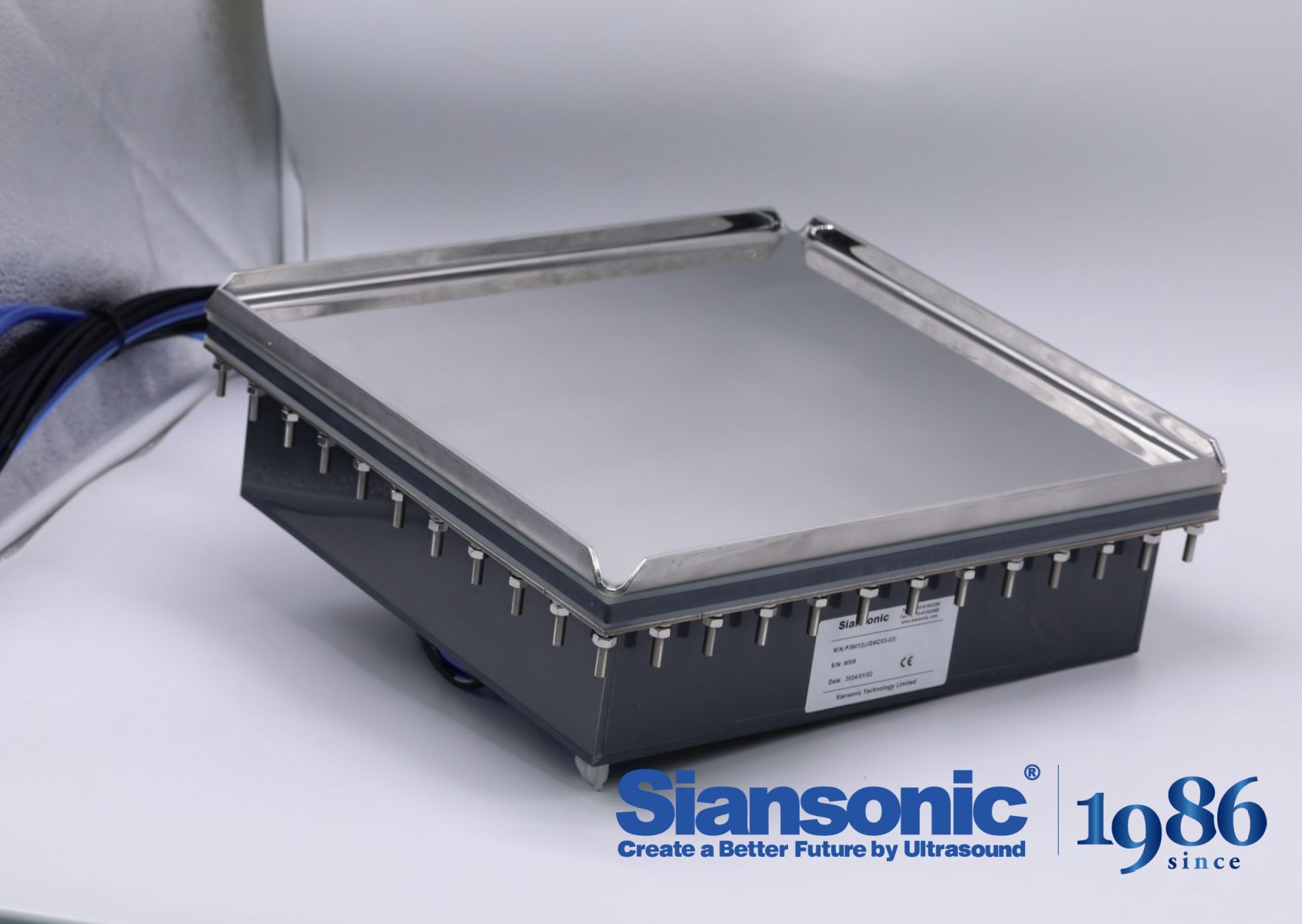
Cleaning narrow pitch and deep trench structures demands more than a fixed ultrasonic frequency. A tailored frequency sweep adjusts the output across a controlled range, preventing standing waves that leave residue in tight gaps. By continuously shifting between high and low cycles, the system targets both micron-scale particles near the surface and stubborn contaminants lodged at the trench bottom.
The sweep profile is configured based on the specific aspect ratio and material of the features. For dense arrays with sub-10 micron spacing, the sweep avoids resonance hotspots that can damage fragile sidewalls. Meanwhile, deep trenches benefit from lower frequency components that generate larger cavitation bubbles, reaching depths that a single frequency would miss entirely.
Operators can store multiple sweep recipes and switch between them without hardware changes. This not only shortens process development time but also enables consistent cleaning results across different wafer layouts. The result is a reproducible, damage-free process that keeps yield high even as device geometries continue to shrink.
Matching Chemistry and Acoustic Energy to Emerging Thin Films
The push toward thinner, more complex films has made it impossible to treat deposition as a simple thermal budget problem. Emerging materials like two-dimensional dichalcogenides, metal-organic frameworks, and ultra-thin high-k dielectrics respond to acoustic energy in ways that standard recipes rarely capture. Acoustic excitation, whether from a piezo-driven nozzle or a substrate-level transducer, shifts the energy landscape at the growing interface. This means chemistry that looks inert in a beaker can become active when a film is assembled under the right frequency and amplitude.
In practice, matching chemistry to acoustic energy means paying attention to molecular relaxation times and solvent evaporation rates. A precursor with a heavy ligand shell may need a lower-frequency acoustic field to avoid cracking the film before it densifies. Conversely, a small, rigid molecule may benefit from higher-frequency agitation that keeps surface adatoms mobile without raising the substrate temperature. The goal isn't more energy; it's the right energy distribution across the liquid-vapor and solid-liquid boundaries.
One underappreciated factor is how acoustic energy changes nucleation density. When a film nucleates too sparsely, the resulting grains grow large and rough. A tuned acoustic field can create more uniform nucleation sites, especially on hydrophobic or patterned surfaces where wetting is uneven. The challenge is that each new film stack has its own acoustic impedance and chemical reactivity, so the matching process has to be treated as a material-specific design step, not a fixed parameter in a vendor manual.
Building Uniform Acoustic Fields Across the Entire Wafer Surface
Achieving a truly uniform acoustic field across a full wafer demands more than simply scaling up transducer dimensions. The core challenge lies in suppressing edge diffraction and standing wave patterns that naturally emerge when acoustic energy meets abrupt physical boundaries. One practical route involves segmenting the piezoelectric source into an array of individually driven elements. By carefully adjusting the phase and amplitude delivered to each segment, the near-field interference can be reshaped so that the resulting pressure distribution flattens out across the wafer plane, even within a few millimeters of the edge. This approach also allows compensation for subtle variations in wafer thickness or coupling layer properties without redesigning the entire acoustic stack.
Another effective strategy focuses on the propagation medium itself. Inserting a gradient-index acoustic matching layer between the transducer and the wafer helps to gradually taper the acoustic impedance, which minimizes reflections that would otherwise create hot and cold spots. Combining this with a convex or stepped lens profile can redirect off-axis energy back toward the periphery, counteracting the natural drop-off in field strength. Finite element simulations play a critical role here: by iterating on lens curvature and matching layer composition, engineers can converge on a design where the peak-to-valley pressure variation across a 300 mm wafer stays within a few percent, even at frequencies above 1 MHz.
Beyond static hardware optimization, real-time field monitoring offers a way to maintain uniformity during processing. By embedding a sparse array of miniature hydrophones or piezoelectric sensors at the wafer chuck periphery, the system can detect deviations from the target acoustic profile. A closed-loop controller then adjusts the excitation signals to the transducer segments, dynamically compensating for temperature drift, acoustic loading changes from dispensed fluids, or mechanical relaxation of the stack. This feedback-driven approach transforms uniformity from a one-time calibration target into a continuously maintained condition, which becomes especially valuable in high-volume manufacturing where wafer-to-wafer repeatability is non-negotiable.
Real-Time Cavitation Control for Damage-Free Ultraclean Results
Real-time cavitation control adjusts ultrasonic energy thousands of times per second, adapting to load shifts, temperature drift, and part geometry. The result is a stable bubble field that never collapses violently enough to erode delicate surfaces, yet still generates the micro-jets needed to strip submicron contaminants from blind holes and complex textures.
Unlike fixed-frequency systems that create hot spots and dead zones, this approach monitors acoustic impedance at the transducer face and modulates amplitude within microseconds. That means oxide films, polishing residues, and fine particulates are removed with consistent uniformity across the entire tank volume, without relying on aggressive chemistry or extended cycle times.
The practical payoff is measurable: zero cavitation-induced pitting on aluminum substrates, no stress corrosion on heat-treated alloys, and repeatable surface energy values after rinsing. Operators spend less time reworking damaged parts or validating cleanliness, because the process stays inside a narrow window where cleaning forces remain below the fatigue threshold of the material.
Integrating Custom Megasonic Modules into Existing Fab Workflows
Merging a custom megasonic module into a fab's established wet bench or single-wafer tool demands more than a simple bolt-on. The module's transducer placement, frequency tuning, and power delivery must align with the existing tank geometry and chemical circulation patterns. If not carefully matched, you end up with uneven cavitation fields that can damage fragile device features. We've seen cases where a supposedly plug-and-play module required re-engineering the entire overflow weir just to maintain proper acoustic coupling.
Beyond the physical footprint, the control architecture rarely talks nicely on day one. Your custom module might speak a dialect of SECS/GEM that the host EAP doesn't fully parse, or it may rely on a standalone PLC that sits outside the tool's recipe tree. The real integration work often lives in the data layer: mapping megasonic power, frequency, and degas status into the tool's existing variable collection so process engineers can actually trace what happened lot by lot.
Practical constraints like DI water flow, exhaust tie-ins, and even floor loading can derail a project if ignored early. Retrofitting a megasonic source often means rerouting ultrapure water lines and adding a dedicated power conditioner. And don't forget about maintenance access—if a technician can't reach the transducer for a quick swap without pulling the entire tank, your uptime numbers will quietly suffer. Planning for those mundane but critical details is what separates a smooth integration from a six-month troubleshooting saga.
FAQ
Ultrasonic baths typically operate below 100 kHz and rely on cavitation, which can transmit enough energy to damage sub-50 nm patterns. A megasonic system works in the 0.8–1.2 MHz range, using acoustic streaming rather than violent bubble collapse. Customization enters through transducer placement, power density, and chemistry delivery so the energy stays uniform across the wafer instead of concentrating near edges.
It removes particles that are too small for brush scrubbing or high-pressure spray without leaving organic residues. The gentle shear forces dislodge particles from recesses and high-aspect-ratio trenches. When combined with dilute chemistries, the process lowers metal contamination and haze levels that directly affect device yield.
Advanced nodes include ultra-thin wafers, bonded stacks, and suspended microstructures. A generic cleaning recipe can fracture these features through mechanical stress or thermal shock. Custom systems allow users to adjust frequency, sweep rate, and liquid flow so the cleaning force stays below the damage threshold of each specific structure.
It handles submicron particles, slurry residues from CMP, metal ions, and organic films. By adjusting chemistry and acoustic energy, the system can target a specific contaminant without attacking the underlying film. For example, dilute ammonia-peroxide mixtures work well for organic residues, while ozonated water handles metal contamination.
The key is controlled fluid flow and rapid rinse steps. Megasonic energy keeps particles suspended in the boundary layer rather than letting them settle back onto the surface. Custom nozzles or overflow weirs direct the particle-laden solution away from the wafer before the rinse begins. Some systems also use point-of-use filtration to reduce the particle concentration in the bath.
Yes, many designs are modular. The transducer and power supply can be adapted to fit a standard tank or a single-wafer spin chamber. Integration usually involves mounting the transducer below a quartz or sapphire window, then tuning the drive signal to the chamber's acoustic properties. This allows existing tools to gain megasonic capability without replacing the entire wet process line.
A fixed frequency creates standing waves with nodes and antinodes, leading to uneven cleaning. Sweeping the frequency over a narrow band, such as ±50 kHz around 1 MHz, shifts these nodes continuously so the acoustic energy averages out across the wafer. This is essential for large-diameter wafers where edge-to-center uniformity affects yield.
These substrates are harder and chemically resistant, but they also carry higher surface charge densities that attract particles. Custom systems can pair megasonic energy with specialized surface-active chemistries and higher power densities to overcome the stronger adhesion. The frequency and flow are adjusted to avoid damaging epitaxial layers or creating subsurface damage in brittle materials.
Conclusion
As device geometries shrink below the point where standard megasonic baths introduce unacceptable damage or fail to dislodge particles from high-aspect-ratio features, custom megasonic wafer cleaning systems step in with precisely engineered acoustic delivery. Rather than relying on fixed-frequency immersion tanks, these systems tailor frequency sweeps to match narrow pitch and deep trench dimensions, preventing destructive standing waves while still imparting enough energy to remove sub-10nm contaminants. Matching the chemistry and acoustic energy to emerging thin films is equally critical; a one-size-fits-all approach often leaves residues on new low-k dielectrics or metal gate materials, so custom tools adjust power density and solvent composition for each film stack.
Building uniform acoustic fields across the entire wafer surface demands careful transducer array design and real-time feedback. Custom systems incorporate multizone transducers and in-situ cavitation sensors that continuously monitor bubble activity, allowing instant adjustments to avoid pattern collapse or surface damage. This real-time cavitation control delivers damage-free ultraclean results even on fragile 3D structures. Finally, integrating these custom megasonic modules into existing fab workflows is streamlined through drop-in chamber designs and software hooks that communicate with factory automation, ensuring that advanced cleaning capability does not disrupt throughput or require a full line requalification.
Contact Us
Contact Person: Ivy Zhang
Email: [email protected]
Tel/WhatsApp: +86 1081502288
Website: https://www.siansonic.com/